Materials
Home . Technical Solutions . Materials
PREV
NEXT
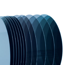
Single Side Polished (SSP) Wafers
Our customized Single Side Polished (SSP) wafers supply a perfect platform for Discrete&Analog applications, surface MEMS, capping etc.
With controlling crystal growing, it provides the foundation for our highly doped, low-resistivity wafers that enable extremely high performing power semiconductors.
Our red phosphorus wafers boast ultra-low resistivity values that reduce the on-resistance and power losses of low-voltage power MOSFETs.
Our red phosphorus wafers boast ultra-low resistivity values that reduce the on-resistance and power losses of low-voltage power MOSFETs.
SSP wafers specifications
Growth Methods |
Cz, MCz |
Diameter |
150, 200mm |
Crystal Orientation |
<100>, <110>, <111>, off-oriented |
N Type Dopants |
Arsenic, Phosphorus, Red Phosphorus |
P Type Dopants |
Boron |
Resistivity |
<1mOhm-cm up to over 5,000 Ohm-cm |
Backside Treatment |
Etched, Polyback, LTO, Polished |
Our Single Side Polished (SSP) wafer in 200 mm diameter is compatible even with the most demanding process lines. It has excellent thickness and flatness capabilities. We also supply SSP wafers with non-standard thickness for special applications (6” 380-1300 µm; 8” 500-1500 µm).
Industries
Advanced Materials Corporation
11F-PH, The AMC Tower, 222, Bongeunsa-ro, Gangnam-gu, Seoul 06135, Korea|TEL : +82-2-526-5900|FAX : +82-2-526-5920|Privacy PolicyAdvanced Materials Corporation
11F-PH, The AMC Tower, 222, Bongeunsa-ro, Gangnam-gu, Seoul, 06135, KoreaTEL : +82-2-526-5900|FAX : +82-2-526-5920
Privacy Policy
COPYRIGHT (C) AMC ALL RIGHTS RESERVED.
DESIGNED BY WAY21
![]()